Link You To Professional Networks

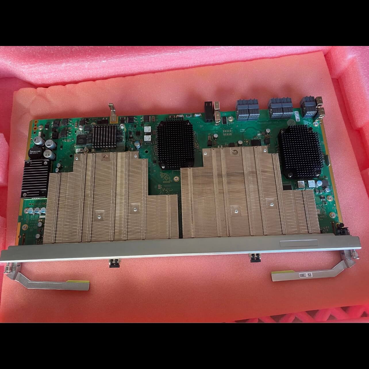
TNSAN502 Is Huawei OptiX OSN 9800 2 Port 200G Line Service Processing Board

Huawei OptiX OSN 9800 2 Port 200G Line Service Processing Board TNSAN502 Overview
TNSAN502: 2 x 200G line service processing board (OTN)
The N502 board is a line board and supports a mixture of OTN and SDH services. The N502 board processes and converts the received service signals into two OTUC2 signals or one OTUC4 signal. The OTUC2 or OTUC4 signals are carried over DWDM wavelengths. The N502 board uses coherent receiving technologies and applies to coherent systems.
The N502 board consists of an ODUk cross-connect module, an OTN processing module, a VC cross-connect module, an SDH processing module, a WDM-side optical module, a control and communication module, and a power supply module.
The transmit and receive directions are defined in the signal flow of the N502 board. The transmit direction is defined as the direction from the backplane to the WDM side of the board, and the receive direction is defined as the reverse direction.
The following describes the signal flow in the transmit direction along with the module functions.
VC-4 signals and ODUk signals can be cross-connected through the backplane.
The VC-4 signals are received by the VC cross-connect module and sent to the SDH processing module for STM-N framing and overhead processing. The generated STM-N signals are sent to the OTN processing module.
The ODUk signals are received by the ODUk cross-connect module and directly sent to the OTN processing module.
The OTN processing module maps the STM-N signals to the payload of appropriate ODUk signals, performs OTN framing and FEC encoding of the signals, and then produces and sends OTU electrical signal to the WDM-side optical module.
The WDM-side optical module receives the OTU electrical signal from the OTN processing module, performs E/O conversion, and sends out one OTU optical signal over a DWDM wavelength through the OUT port.
The N502 board electrically regenerates one OTU optical signal, which are carried over DWDM wavelengths at both the transmit and receive ends.
The optical receiver receives the optical signals to be regenerated through IN optical ports and converts them into electrical signals.
The OTN processing module performs FEC decoding, overhead processing, and FEC encoding, which is the process of reshaping, regenerating, and retiming the electrical signals and mapping them into OTN-frame signals.
The OTN processing module then sends the OTN-frame signals to the optical transmitter. After performing E/O conversion, the optical transmitter produces and sends out OTU optical signals over DWDM wavelengths through the OUT port.
Functions and Features of the TNSAN502 Board
|
Function and Feature |
Description |
|
Basic function |
Provides two line ports and supports conversions between a maximum of 320 ODU0 signals, 320 ODUflex signals, 160 ODU1 signals, 40 ODU2(e) signals, 8 ODU3 signals, or 4 ODU4 signals and 2 OTUC2/1 OTUC4 signals. For details about the service mapping path, see Application. |
|
Backplane capacity |
The maximum capacity is 400 Gbit/s. |
|
WDM specification |
Supports the DWDM specifications. |
|
Tunable wavelength |
Supports tunable wavelengths of WDM-side optical signals in Super C band (1524 nm to 1573 nm). |
|
FEC coding |
SDFEC2 |
|
Line modulation format |
200G line mode:
400G line mode:
|
|
Typical channel spacing |
|
|
OTN overhead |
200G line mode:
400G line mode:
|
|
Intra-board 1+1 protection |
Supported NOTE:
|
|
ODUk SNCP |
Supported |
|
Tributary SNCP |
Supported |
|
Electrical-layer ASON |
Supported |
|
Optical-layer ASON |
Supported NOTE:
|
|
Digital optical label |
When LS Ability is enabled, the board supports loading low-frequency pilot-tone modulation signals and overheads during wavelength conversion, and can work the optical-layer board that supports the digital optical label function to detect optical power and overheads and report optical performance data. |
|
Physical clock |
Supported NOTE: When the ODU cross-connect granularity of an OTN line port is set to the maximum granularity supported by the port, physical clock synchronization is not supported. The physical clock can be used only after lower-order ODU cross-connections are configured. |
|
IEEE 1588v2 |
Not supported |
|
ITU-T G.8275.1 |
Not supported |
|
ITU-T G.8273.2 |
Not supported |
|
Outband DCN |
Supports communication over ESCs. |
|
Test frame |
Not supported |
|
PRBS |
Supports the PRBS function on the WDM side. |
|
Latency measurement |
The board supports latency measurement in the WDM-side optical port direction (upstream direction)
NOTE: When VPs are configured, the board supports measuring the PM/TCM latency of higher-order and lower-order ODUk channels. |
|
Channel loopback |
ODUk (k=0, 1, 2, 2e, 3, 4, flex) channel loopbacks |
|
Port loopback |
Supports WDM Side Loopback |
|
Alarm and performance event monitoring |
|


